Odpověď na názor
Odpovídáte na názor k článku Budoucnost čipové technologie: TSMC odhalilo 1,6nm proces, Super Power Rail bude přelomová změna. Názory mohou přidávat pouze registrovaní uživatelé.
-

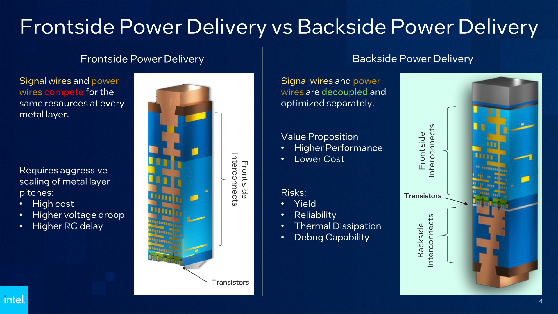
the trade-off for all of this is primarily in losing the previously mentioned perks of building a frontside chip. The transistor layer is now roughly in the middle of the chip, rather than at the end. This means that traditional debugging tools can’t directly poke the transistor layer of a completed chip to test it, and there is now 15 or so layers of signal wires between the transistor layer and the cooling service. These aren’t insurmountable challenges, as Intel’s paper takes care to lay out, but were issues that Intel had to work around in their design.
Manufacturability is the other set of trade-offs involved in moving to BS-PDN. Building power layers on the backside of a die is something that’s never been done before, which increases the chance of something going wrong. So not only does power delivery need to work, but it needs to work without significantly reducing chip yields or otherwise making chips less reliable. But if all of these things pan out, then the extra effort of building power layers on the backside of a wafer are more than cancelled out by the time and cost savings of not having to route power in through the front side.
https://images.anandtech.com/doci/18894/PowerVia%20Technical%20Deck_04.png
je to sice od Intelu ale pro TSMC budou platit ta stejná omezení


Návody a tipy

 23. 10. 2024
| online
23. 10. 2024
| online
 31. 7. 2024
| online
31. 7. 2024
| online

 6. 7. 2024
| online
6. 7. 2024
| online


